


Servicios Personalizados
Articulo
 pdf en Inglés
 Articulo en XML
 Referencias del artículo
 Permalink
Latin American applied research
versión On-line ISSN 1851-8796
Lat. Am. appl. res. vol.43 no.2 Bahía Blanca abr. 2013
Analysis of the influence of switching related parameters in the dab converter under soft-switching
G. G. OGGIER †, G. O. GARCIA †andA. R. OLIVA†‡
†Grupo de Electróonica Aplicada(GEA), Facultad de IngenierÃa, Universidad Nacional de RÃo Cuarto, Ruta Nacional # 36 Km. 601, X5804BYA, RÃo Cuarto, Argentina. CONICET goggier@ing.unrc.edu.ar
‡ Instituto de Investigaciones en IngenierÃa Eléctrica “Alfredo Desages”, Dpto. de Ing. Eléc. y de Computadoras, Universidad Nacional del Sur, BahÃa Blanca, Argentina. CONICET. aoliva@uns.edu.ar
Abstract— An analysis of a dual active bridge (DAB) converter under soft-switching mode in the whole operating range is presented in this paper. A detailed study of the impact of the transformer magnetizing inductance, LM, and snubber capacitance, Cxx, parameters on the soft-switching regions is carried out to obtain some design considerations. Simulation and experimental results which validate the theoretical analysis are also presented.
Keywords— dc-dc converters, dual active bridge converter, soft switching, modulation strategy.
I. INTRODUCTION
Thedual activebridge(DAB) converter issuitablefor applications that require high-power isolated DC-DC converters(Ionue and Akagi, 2007). The main characteristics of theDAB converter arehighpowerdensity, operation under soft-switching mode andbidirectional and simple power flow control(DeDoncker et al., 1991; Xie et al., 2010). The DAB converter operating characteristics as well as a comparison with other topologies can be found in Steigerwald et al. (1996), Taoet al. (2008) and,Krismer andKolar(2010).
For those applications that require a wide voltage ratio,asfor instanceenergy storagesystems,fuel cells, photovoltaic applications, etc. (Wanget al., 2007;Camara et al., 2010),theDAB converter isan interesting option but it presents a reduced soft-switching operating range limited to high output currents when the conventional modulation strategy(CMS) is used(Inoue and Akagi, 2007).
In Kheraluwala et al. (1992) it is considered the effects of the transformer magnetizing inductance and snubber capacitance on the operation of theDAB con-verter, concluding that these parameters significantly affect the soft-switching region.
In order to extend the operation range under soft-switching mode different modulation strategies are proposed(Oggier et al., 2006 and Jain and Ayyanar, 2008).
In Oggier et al. (2011) a new modulation strat-egy(NMS) to operatetheDAB converter under soft-switching in the whole operating range and minimize thereactivepowertoreducetheconduction losseswas proposed.
In this paper a similar analysis is presented but including the transformer magnetizing inductance and the snubber capacitance parameters . This analysis allows establishing guidelines for sizing these parameters inordertoallowtheDAB convertertooperateunder soft-switching mode in the whole operating range. Simulation and experimental results are included to validate the analysis.
The paper is organized as follows. Section I containsan introduction. SectionIIpresentsapower flow analysis using the NMS. The converter operation under soft-switching mode in its whole operation range is analyzed in Section III. The same section also containsguidelinesfor sizing the transformer magnetizing inductance and snubber capacitance. Simulation and experimental results are given in Section IV. Finally, conclusions are drawn in Section V.
II. POWER FLOW ANALYSIS
A. Modulation Strategy
The NMS consists of driving the bridge with the largestdc voltage togenerate a three-levelPWM voltage waveform while the other bridge generates a constant frequency voltage square waveform with 50% duty cycle (Oggier et al., 2006; Oggier et al., 2009).
The direction of the required output power can be controlled by manipulating the phase-shift, δ, between the voltages of the transformer terminals, υT1 and υT2, and the modulation index, m, applied to the bridge which is fed with the largest dc voltage.
The analysis presented in this paper considers the influence of the transformer magnetizing inductance on the operation of the DAB converter when the NMS is used. Figure 1 shows an equivalent circuit referred to the primary side of the converter. The high-frequency transformer was modeled by using an equivalent T model, with leakage inductance split equally on each side of the finite magnetizing inductance. Winding resistances are considered negligible. Let the magnetizing inductance be LM = KL, where L is the total leakage inductance and 1 ≤ K ≤ ∞, expressing the extreme values for the magnetizing inductance. In order to simplify the analysis, the transformer turns ratio will be considered hereinafter equal to 1 and the value of K will be constant when the core of the highfrequency transformer is not saturated.
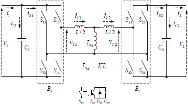
Figure 1: DAB converter simplified scheme.
Figures 2(a) and 2(b) show the ideal waveforms for the DAB converter operating at V1 > V2 (buck mode), power flowing from V1 to V2 and K < ∞. Bridge B1 is driven to modulate υT1 and two particular cases are shown: δ ≥ 0º and δ < 0º. In these Figures, δ is the phase shift between υT1 and υT2, β1 and β2 correspond to current zero crossings iT1 and iT2, respectively, α is the angle at which iT1 reaches its maximum value, and τ is the width of the pulse generated by the bridge fed with the largest dc voltage ( τ = π for the CMS).
Figure 2: Ideal voltages and current waveforms for K < ∞: (a) buck mode for δ ≥ 0º and ; (b) buck mode for δ < 00; (c) boost mode for δ ≥ 00 and (d) boost mode for δ < 00.
Figures 2(c) and 2(d) show similar information for the DAB converter operation for V1 < V2 (boost mode), now B2 is driven to modulate υT2. In this operating mode α is the angle at which iT2 reaches its maximum value.
All the cases shown in Fig. 2 correspond to the DAB converter operating under ZVS soft-switching mode (Bellar et al., 1998) and they are used to determine the DAB converter soft-switching constraints.
B. Converter output power
In this Subsection, the DAB converter output power is analyzed in order to obtain the expressions to obtain the output power.
Let us consider the simplified model shown in Fig. 1, the currents iT1 e iT2 can be expressed as
 | (1) |
 | (2) |
where θ = ωt, ω = 2πfs, fs is the switching frequency, K1 = (1 + 1/ (2K)) / (ωL(1 + 1/ (4K))) and K2 = 1/ (ωL(1 + 1/ (4K))).
By solving iT1 and iT2 in (1) and (2) for each operation mode and switching intervals defined in the Fig. 2(a) y Fig. 2(b) for the buck mode, the expressions shown in Table 1 can be obtained, where α = τ and α = π â τ + δ for buck and boost operation mode, respectively
Table 1: Expressions to represent iTx for each interval and operating mode.
where KA = K1 and KB = K2 for iT1 and KA = K2 and KB = K1 for iT2.
The DAB converter average output power can be obtained, for both buck and boost operating modes by solving the following expression
 | (3) |
where x = 1 or 2 corresponding to bridge 1 or 2, respectively.
By solving (3), the following expressions can be obtained as a function of the feeding voltage, V1, for δ ≥ 0º
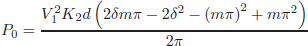 | (4) |
and for δ < 0º
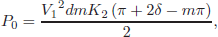 | (5) |
where d is the DAB voltage conversion ratio, V2/V1, m is the modulation index of the corresponding bridge, defined as m = τ/π (Oggier et al., 2006).
Equations (4) and (5) are valid for both buck and boost operation modes. It can be deduced from these expressions that the output power can be controlled by manipulating both variables: δ and m.
From (4) and (5) it can be determine the following expression to calculate δ as function of the power flow to be transferred as follows:
For δ ≥ 0º
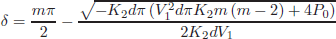 | (6) |
and for δ < 0º
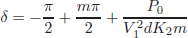 | (7) |
III. SOFT-SWITCHING OPERATION
A. Soft-switching restrictions
This Section contains an analysis of the DAB converter operation under soft-switching mode considering the effect of the transformer magnetizing inductance and the snubber capacitance on the soft-switching region. Thus, it will be demonstrated that it is possible to operate the converter under soft-switching in its whole operation range by adequately manipulating the variables δ and m and designing the high-frequency transformer in order to obtain a magnetizing inductance able to reduce the negative effect of snubber capacitance on the soft-switching region (Kheraluwala et al., 1992).
When the converter operates under soft-switching, the following inequalities must be fulfilled (DeDoncker et al., 1991):
 | (8) |
and
 | (9) |
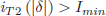
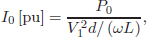
where Imin is the minimum current which ensures ZVS operation; that is the minimum current that ensures that the voltage across the power transistor (Txx in Fig. 1) reaches the clamping value Vx at the same time current reaches zero. In Kheraluwala et al. (1992) it was determined that this current can be expressed as
 | (10) |
where ωn = ω0/ω, ω = 2πfs, 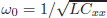 and Cxx is the snubber capacitance (see Fig. 1). The last expression was normalized respect to a base value defined as V1/ (ωL).
Inequalities (8) and (9) determines the soft-switching limits for bridges B2 and B1, respectively (DeDoncker et al., 1991; Oggier et al., 2006).
Evaluating (8) and (9) using expressions in Table 1, the restrictions for operation under soft-switching shown in Table 2 can be obtained for both bridges and both operation modes, where conditions 1 and 2 represent iT2 (δ) > Imin and iT1 (π) > Imin when δ ≥ 0º, respectively, and conditions 3 and 4 iT2 (δ) > Imin and iT1 (π) > Imin when δ < 0º, respectively. These restrictions determine the limits of the variable δ, as a function of d, m, K and Imin, and allow determining the range of output power for which the DAB can operate under soft-switching.
Table 2: Restrictions for operation under soft- switching.
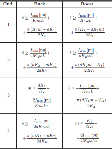
Figure 3 shows the limits for A and B soft-switching regions in the plane d as a function of I0[pu] for different values of K where
 | (11) |
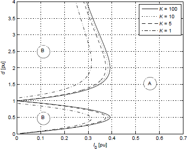
Figure 3: Soft-switching regions as a function of d and I0[pu] with K as parameter.
A)- Soft-Switching region for δ ≥ 0º.
B)- Soft-Switching region for δ < 0º.
yielding
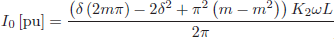 | (12) |
In this Figure, area A represents the soft-switching operation region for δ ≥ 0º, whereas area B represents the soft-switching operation region for δ < 0º. In both regions the manipulating variables are chosen so that they fulfill the soft-switching restrictions. Boundaries between regions A and B are obtained by evaluating (12) with the restrictions in Table 2 for δ = 0º and m = d, if d < 1 or m = 1/d if d > 1.
By analyzing the expressions given in the Table 2 it can be concluded that the adopted modulation indexes for δ = 0º are not the only possible values that fulfill the constraints (8) and (9). It can be demonstrated by using the current expressions iT1 and iT2 given in Table 1 that iT1 (π) = iT2 (δ) for each K with the proposed modulation index. In other case, one of the current at the switching angle is lower than that obtained with the proposed modulation index, resulting in the most unfavorable situation to achieve soft-switching conditions (Bellar et al., 1998).
From this analysis it can be concluded that the modulation strategy consists of choosing the values of δ and m that fulfill the restrictions given in Table 2.
B. Design considerations
This section establishes guidelines for sizing the transformer magnetizing inductance and snubber capacitance. These guidelines are based on the fact that Cxx reduces the soft-switching operation region, whereas the magnetizing inductance tends to increase it (Kheraluwala et al., 1992). It suggests that it might be useful to know the best combination of these two parameters that guarantees soft-switching conditions in the whole operation range for both modes.
It can be demonstrated that turn-off losses of the DAB converter decrease proportionally with Cxx (Oggier et al., 2009). Thus, Cxx can be estimated as a function of the requirements for turn-off losses by using the following expression derived in McMurray (1980)
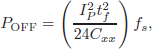 | (13) |
where IP is the magnitude of the current at the beginning of the switching time and tf is the time at which the current becomes zero. Once selected the value of Cxx, it must determine the value of K.
To ensure that the converter operates under soft-switching the current at the switching angles must exceed a certain minimum value given by (10). In previous section, it was shown that when the converter operates within the boundaries of regions A and B, Fig. 3, the currents iT1 and iT2 at the switching angles δ and π reach their minimum values, being the most unfavorable situation to operate under soft-switching.
Figure 4 shows the magnitude of this current in pu when the converter operates within the boundaries of regions A and B (δ = 0º and m = d if d < 1 or m = 1/d if d > 1) as a function of d and K as parameter, as it was explained in the previous section. This Figure shows that for buck mode the magnitude of the switching current increases linearly with d, whereas for boost mode it is independent of this value. Thus, it can be concluded that boost operation mode is more favorable to optimize the design of the DAB converter.
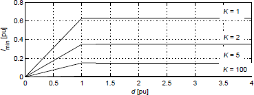
Figure 4: Minimum current at the switching angles as a function of d with K as parameter. (δ = 0º and m = d if d < 1 or m = 1/d if d > 1).
Figure 4 shows that the switching current increases when K → 1; this allows increasing the size of snubber capacitance and consequently lead to lower turnoff losses. On the other hand, from the Eqn. (12) can be deduced that if K → 1 the maximum output current that can be obtained decreases. As a conclusion, in order to minimize switching losses, the magnetizing inductance must be maximized up to the value that allows the converter to transfer the maximum required output power. The maximum value of Lm can be obtained by solving K from (12), when δ = π/2 and I0 [pu] = I0max [pu].
After selecting the snubber capacitance from (13), the value of K can be obtained matching (10) with the current expressions iT2 (θ) or iT1 (θ) shown in the Table 1 at the angles δ or π, respectively, for δ = 0º and m = d if d < 1 or m = 1/d if d > 1. Thus, the following expressions can be obtained:
For buck modes
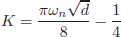 | (14) |
and for boost mode
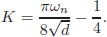 | (15) |
Finally, a minimum dead-time has to be determined. This dead-time should be chosen conservatively so as to be grater than the maximum time of charge/discharge of the snubber capacitante of the power transistors to avoid cross conduction (Mohan et al., 2003). To do this, it can be used the following expression (Kheraluwala et al., 1992)
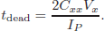 | (16) |
In the next section, simulation and experimental results to validate the previous analysis are presented.
C. Determination of the modulation index and phase-shift
In Bai and Mi (2008) it is shown that when using the CMS a considerable portion of the current is used just to generate reactive power and not contributing with the active power flow, resulting in an unnecessary electrical stress on the semiconductor switches and a lower efficiency, especially under light-load operation.
An algorithm to minimize the reactive power through the transformer represented by L is proposed in Oggier et al. (2011); the parameter K is considered infinite. From this analysis the values of δ and m are obtained as a function of the converter operating point, d and I0[pu].
The reactive power through L can be defined as
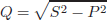 | (17) |
where P is the average active power, that is equal to zero in a switching period, and S is the apparent power determined as
 | (18) |
where
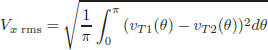 | (19) |
and
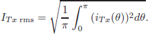 | (20) |
Voltages υT1 and υT2 can be deduced from the waveforms shown in Fig. 2 to evaluate (19), while the expressions for current iTx shown in Table 1 can be used to evaluate (20). For space reasons are not included here the expressions of reactive power.
Figure 5 shows the calculated level curves for m that minimize the reactive power as functions of I0[pu] and d. Thus, the value of m can be determined for each DAB converter operating point by implementing a two-input table. Modulation values shown in Fig. 5 correspond to normalized values which are independent of the DAB converter parameters.
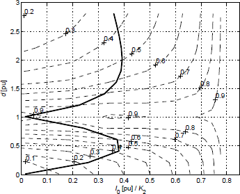
Figure 5: The dashed lines correspond to level curves showing the values of m that minimize the reactive power in the plane d versus I0[pu]. The solid line corresponds to the boundaries of regions A and B.
After determining the value of m, variable δ must be calculated according to (6) or (7) when the DAB converter operating point belongs to regions A or B in Fig. 3, respectively.
IV. RESULTS
In this section simulation and experimental results are presented to validate the theoretical hypotheses presented in the previous Sections. Results are presented only for boost operation mode.
The experimental DAB converter parameters can be summarized as follow: Maximum output power P0max = 2kW, switching frequency fs = 20kHz, output voltage V2 = 120V, K = 7.5, Cxx = 1nF and transformer turns ratio n = 2.5. The power switches were implemented using IGBTs and the highfrequency transformer was built using a ferrite core. In order to simplify the implementation, an external inductor of L = 20µHy was added.
A. Simulation results
In order to verify the operation of the converter under soft-switching mode, simulation results on the boundary between regions A and B for the particular case d = 2 are presented.
Figure 6(a) shows the waveforms of the transformer terminal voltages υT1 and υT2 and currents iT1 and iT2 referred to one side of the converter. This figure shows that the currents iT1 and iT2 in the times equivalent to angles π and δ are positive. Thus, according to the analysis realized in the previous section, the DAB converter operates under soft-switching.
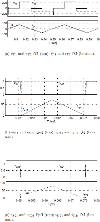
Figure 6: Simulation results corresponding to the op- eration on the boundaries between region A and B of Fig. 3 for d = 2.
Figure 6(b) shows the waveforms of voltage terminals, vS11, gate voltage, vG11 of the switch S11 and currents through the power transistor T11 and diode D11. It can be observed that the transistor turn-on signal is established when the diode is in conduction state. When the current crosses zero, turn-on of the transistor occurs under zero-voltage-switching condition (Bellar et al., 1998). Figure 6(c) shows the waveforms of voltage terminals, vS21, and gate voltage, vG21 of the switch S21 (top) and current waveforms through the power transistor T11 and diode D11 (bottom), similar to Fig. 6(b). These results allow to validate validate the soft-switching operation of both bridges.
B. Experimental results
The DAB topology using the conventional modulation strategy (CMS) can operate under soft-switching but only within a reduced range of operation, depending on the voltage conversion ratio and on the output current. This is an important drawback for some applications that operate most of the time with variable or low load because the overall efficiency is reduced.
In this paper overall efficiency measurements are shown in order to demonstrate that by using the NMS a higher performance is possible, including variable voltage conversion ratio and different levels of output power.
Figure 7 show the experimentally measured efficiency versus the converter output power for three different values of the voltage conversion ratio using the NMS. It can be concluded from these Figures that the efficiency remains at a high and constant value in the whole range of the output power.
Figure 7: Efficiency versus the DAB converter output power using the NMS for three different values of voltage conversion ratio d = 1.5, 1.75 y 2.0.
With the aim of separating switching and conduction power losses in Figure 8 are shown experimental waveforms of the υCE (Ch1), iSwitch (Ch2) of the switch S21 and the results of multiplying channel 1 and channel 2 (Bottom), corresponding to instantaneous power dissipation, using the NMS for a voltage conversion ratio d = 1.5 and P0 = 1.5 kW (I0[pu] = 0.7).
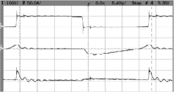
Figure 8: Experimental waveforms corresponding to vCE S21 (Ch1), iS21 (Ch2) and the instantaneous power dissipation (Bottom: 500W/Div) using the NMS for a voltage conversion ratio d = 1.5 and P0 = 1.5 kW.
In order to contrast previous experimental results related to conduction losses and switching losses, they are evaluated using the expressions derived in Oggier et al. (2009). Figure 9 the results from this evaluation for conduction losses (solid line) and switching losses (dashed line) versus the DAB converter output power using the NMS for three different values of voltage conversion ratio d = 1.5, 1.75 and 2.0. From these results it can be graphically calculated that conduction losses and switching losses are around 60 W and 50 W, respectively, which means that the experimental results are in close agreement with evaluation results.
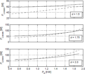
Figure 9: Conduction losses (solid line) and switching losses (dashed line) versus the DAB converter output power using the NMS for three different values of voltage conversion ratio d = 1.5, 1.75 y 2.0.
Figure 10 and Fig. 11 show the experimental waveforms when d = 1.2 and I0[pu] = 0.18 corresponding to iL (Ch3), vCE (Ch1) and vGate (Ch2) of S11 and S21, respectively. In these figures can be observed that the gate signals are activated when antiparallel diodes are conducting, corresponding to a ZVS operation.
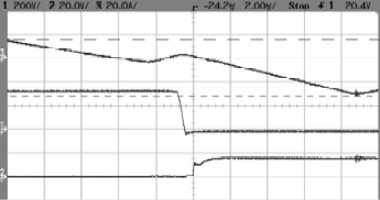
Figure 10: Turn-on experimental waveforms corresponding to iL (Ch3), vCE (Ch1) and vGate (Ch3) of S11.
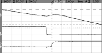
Figure 11: Turn-on experimental waveforms corre- sponding to iL (Ch3), vCE (Ch1) and vGate (Ch3) of S21.
V. CONCLUSIONS
In this paper the operation under soft-switching mode of the DAB converter considering the effect of the transformer magnetizing inductance, LM, and the snubber capacitance, Cxx, which have a significant impact on the soft-switching region (Kheraluwala et al., 1992), was analyzed. From this analysis, the relationships to determine the value of LM and Cxx in order to allows the operation of the DAB converter under soft-switching mode in the whole operating range were obtained. It was proposed that Cxx has be sized according to the requirements of turn-off losses and LM to fulfill the soft-switching constraints. To validate the analysis, simulation and experimental results were obtained. The experimental results demonstrate that it is possible to obtain a high efficiency for variable voltage conversion ratio of the DAB topology, especially in applications at which it operates with variable power, using the proposed strategy.
REFERENCES
1. Bai H., and C. Mi, "Eliminate reactive power and increase system efficiency of isolated bidi- rectional dual-active-bridge dc-dc converter us- ing novel dual-phase-shift control," IEEE Trans. Power Electron., 23, 2905â2914 (2008).
2. Bellar M. D., T. S. Wu, A. Tchamdjou, J. Mahdavi, and M. Ehsani, "A review of soft-switched dc-ac converters," IEEE Trans. Ind. Applications., 34, 847-860 (1998).
3. Camara M. B., H. Gualous, F. Gustin, A. Berthon and B. Dakyo, "DC/DC converter design for su- percapacitor and battery power management in hy- brid vehicle applicationspolynomial control strat- egy,"IEEE Trans. Industrial Electron., 57, 587-597 (2010).
4. De Doncker R. W., D. M. Divan and M. H. Kher- aluwala, "A three phase soft-switched high-power- density dc/dc converter for high-power applica- tions," IEEE Trans. Ind. Applications., 27, 63-73 (1991).
5. Inoue S. and H. Akagi, "A bidirectional isolated dc-dc converter as a core circuit of the next-generation medium-voltage power conversion system," IEEE Trans. Power Electron., 22, 535-542 (2007).
6. Jain A. K and R. Ayyanar, "PWM control of dual active bridge: comprehensive analysis and experi- mental verification," Proc. 34th IEEE IECON, Or- lando, FL, 909â915 (2008).
7. Kheraluwala M. H., R. W. Gascoigne, D. M. Divan and E. D. Baumann, "Performance characteriza- tion of a high-power dual active bridge dc-to-dc converter," IEEE Trans. Ind. Applications., 28, 1294-1301 (1992).
8. Krismer F. and J. W Kolar, "Accurate power loss model derivation of a high-current dual active bridge converter for an automotive application ," IEEE Trans. Industrial Electron., 57, 881â891 (2010).
9. McMurray W., "Selection of snubbers and clamps to optimize the design of transistor switching convert- ers," IEEE Trans. Ind. Applications., 1A-16, 513- 523 (1980).
10. Mohan N., T. M. Undeland andW. P. Robbins, Power Electronics: Converters, Applications, and Design, Wiley, New York (2003).
11. Oggier G. G., R. Leidhold, G. O. Garc´ıa, A. R. Oliva, J. C. Balda, and F. Barlow, "Extending the zvs operating range of dual active bridge high-power dc-dc converters," Proc. 37th IEEE Power Elec- tron. Spec. Conf., Jeju, Korea, 2471-2477 (2006).
12. Oggier G. G., G. O. Garc´ıa, A. R. Oliva, "Switching Control Strategy to Minimize Dual Active Bridge Converter Losses," in IEEE Trans. Power Elec- tron., 27, 1826â1838 (2009).
13. Oggier G. G., G. O. Garc´ıa, A. R. Oliva, "Modulation strategy to operate the dual active bridge dc-dc converter under soft-switching in the whole oper- ating range," IEEE Trans. Power Electron., 26, 1228â1236 (2011).
14. Steigerwald R., R. W. De Doncker, and M. Kher- aluwala, "A comparison of high-power dcdc soft- switched converter topologies," in IEEE Trans. Ind. Appl., 32, 1139â1145 (1996).
15. Tao K. H., J. L. Duarte and M. A. Hendrix, "Transformer-coupled multiport zvs bidirectional dc-dc converter with wide input range," in IEEE Trans. Power Electron., 23, 771-781 (2008).
16. Wang X., F. Tian and I. Batarseh, "High efficiency parallel post regulator for wide range input dc-dc converter," IEEE Trans. Power Electron., 23, 852- 585 (2007).
17. Xie Y., J. Sun, and J. S. Freudenberg, "Power Flow Characterization of a Bidirectional Galvanically Isolated High-Power DC/DC Converter Over a Wide Operating Range," IEEE Trans. Power Elec- tron., 25, 54â66 (2010).
Received: January 2, 2012
Accepted: July 28, 2012
Recommended by Subject Editor: José Guivant
