


Servicios Personalizados
Articulo
 pdf en Inglés
 Articulo en XML
 Referencias del artículo
 Permalink
Latin American applied research
versión On-line ISSN 1851-8796
Lat. Am. appl. res. vol.43 no.3 Bahía Blanca jul. 2013
Post-compensation of a CT first-order ΣΔ ADC using PWL dynamic system
C. Schmidt†, J.E.Cousseau†, J. L.Figueroa†, R. Wichman‡ and S. Werner‡
† Instituto de Investigaciones en Ingeniería Eléctrica "AlfredoDesages",UNS-CONICET, Avda. Alem 1253,
8000 Bahía Blanca, Argentina. Email: cschmidt@uns.edu.ar
‡ Department of Signal Processing and Acoustics, Aalto University School of ElectricalEngineering, P.O. Box 13000, FIN-00076 Aalto, Finland
Abstract — An approach for compensating non-linearities in a continuous-time first-order sigma-delta converter with one bit quantization is presented. The proposed compensators are parallel nonlinear dynamic systems using piecewise linear static functions. A reduction of an order of magnitude is obtained in the measured squared error when compared to the uncompensated sigma-delta converter. Our results confirm a significant improvement in signal to noise and distortion ratio for single tone input signals and in spurious free dynamic range for multi-tone inputs.
Keywords — Analog to Digital Converters; Nonlinearities; PWL Models; Compensation.
I. INTRODUCTION
Recently, the need for high resolution analog to digital converters (ADCs) with low power consumption, especially for mobile applications, has drawn much attention towards sigma-delta architectures for signal conversion. Such devices combine low resolution quantization with oversampling and noise shaping in order to reduce the in-band noise and thus increase the dynamic range. In particular, continuous-time (CT) sigma-delta modulators (SDMs) seem to be an attractive choice because of their inherent anti-aliasing properties and low circuit complexity, among other advantages (Van der Plassche, 2003). Sigma-delta structures have been proposed for many applications, including digital video broadcasting-terrestrial (DVB-T; see Ryan and Mahdi, 2009; Bonizzoni et al., 2008; Jeong et al., 2008) and Bluetooth (Yang et al., 2009). In addition, they provide a flexible choice between resolution and bandwidth, which makes them suitable for multi-standard transceiver architectures combining for example GSM/WLAN/Bluetooth (Morgado et al., 2006; Jose et al., 2007).
Despite of the attractive properties, non-ideal circuit behavior degrades the overall performance resulting in harmonic distortion and increased in-band noise, which reduces the effective number of bits (ENOB) in the converter. A possible solution to reduce this distortion is to use model-based digital post-compensation techniques. These techniques generally consist on applying certain nonlinear dynamic function at the output of the converter such that the distortions originated by non ideal behavior of the device would be cancelled out (Vito et al., 2007; Irons et al., 1991). First, the post-compensator is trained (off-line) using measurement data from the CT SDM. Then, the identified compensator is implemented on-line during normal operation. This methodology involves some extra digital processing, i.e., a few multiplications and additions in the digital domain to obtain the corrected output sample.
In order to obtain an adequate structure for the compensator it is first necessary to understand the non-ideal behavior of CT SDMs. In Schmidt et al. (2011), it is shown that sigma-delta converters (SDCs) present weak nonlinearities and allow for a Volterra representation. Thus, they can be p-linearized with a Volterra system of similar complexity to that of the SDC model (Schetzen, 1980). In Schmidt et al. (2011), parallel polynomial dynamic systems belonging to the Volterra model family are proposed as compensators. Here, we explore the viability of piecewise linear (PWL) dynamic systems with efficient structure to keep the amount of parameters low. We show that the results in harmonic cancelation and signal to noise and distortion ratio (SINAD) improvement are good and also consistent with previous results.
The paper is organized as follows. In Section II models for a CT SDM are presented. The main contribution of this article, i.e. the proposed compensator is described in Section III. Section IV described the simulation results and the paper ends in Section V with some conclusions.
II. MODELS OF A CT SDM
A. Behavioral model
The general hypothesis behind a post-compensation strategy using a finite Volterra model considers that the SDM behavior is well described by a weakly nonlinear system.
We start from the ideal SDM shown in Fig. 1 consisting of three blocks (integrator, quantizer and digital to analog converter (DAC)) connected in a feedback loop. In Schmidt et al. (2011), we consider a model for each block introducing the real effects that preclude SDM ideal behavior, and we find an equivalent block oriented model, illustrated in Fig. 2, that represents the non-ideal SDM. In the diagram P(⋅) and N(⋅) represent weak static nonlinearities and I(s) and H(s) represent linear finite impulse response (FIR) dynamic blocks.
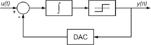
Figure 1: Block diagram of an ideal CT SDM
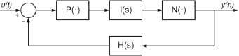
Figure 2: Equivalent block diagram of a CT SDM replacing all elements with their corresponding models.
The integrator in the SDM, as discussed in Leuciuc (2001), can be replaced by a third order polynomial P(⋅) followed by an ideal integrator (i.e., a linear filter I(s)). Also, the DAC in the feedback loop can be represented by a filtered version of the output signal y(t) through a linear filter H(s) (Karema et al., 1991). In addition, the quantizer can be considered almost linear in the signal bandwidth, and so we can model it with a weak static nonlinearity N(⋅).
Hence, the inclusion of non-ideal effects in the block diagram of Fig. 1, leads to the complete behavioral model depicted in Fig. 2. Note that aging and temperature dependencies are not considered at the moment such that the parameters of the SDC remain constant. Based on the behavioral model in Fig. 2, we shall in Section III consider efficient post-compensation techniques for reducing the nonlinear distortion.
B. Circuit model
In order to validate the behavioral model, a circuit model of a CT SDM is simulated in Spice. This circuit model is also used to generate input-output data for the design of two different post-compensators and for the estimation of the parameters involved.
The proposed post-compensation method is calibrated using signals obtained from a transistor level circuit model by transient simulations in Spice. This provides realistic simulation data, leading to general and reliable results when evaluating compensation performance. It also allows to verify which compensation model fits better the physical phenomena that cause the non-ideal behavior.
The circuit model of a first-order CT sigma-delta modulator (SDM) is shown in Fig. 3. Higher order architectures can be obtained by combining several first order SDMs into a MASH structure, with the advantage that the inherent stability of a first-order modulator is preserved. In a MASH structure, the quantization error of a first order SDC is fed to a subsequent first order SDC in order to increase the noise shaping effect without the need of several integrators in the same feedback loop, thus avoiding instability issues (Van der Plassche, 2003).
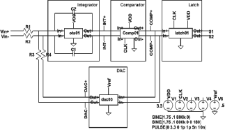
Figure 3: Circuit model of a SDM simulated in Spice. The architecture is fully differential and uses 180 nm CMOS technology.
Our device under test (DUT) has a sampling frequency of 100 MS/s, over a bandwidth from DC to 1 MHz, determining an over-sampling ratio OSR > 50 and a resolution of over 7 bits. Return-to-zero (RZ) coding is used in the feedback loop, which is known to reduce errors in the modulation (Van der Plassche, 2003). A latch outside the loop codes the signal in non return-to-zero (NRZ) format. The architecture is fully differential and the design uses 180 nm CMOS technology with the transistor model provided by manufacturer MOSIS.
In our simulation studies, different sinusoidal single-tone and multi-tone input signals are used to excite the circuit, as usually found in the literature (Nikaeen and Murmann, 2009; Lundin, 2005; Björsell, 2007).
III. PROPOSED COMPENSATOR
The post-compensation scheme proposed in this work is illustrated in Fig. 4, where the SDM block represents the DUT and the ideal SDM is the one represented by Fig. 1. The signal u(t) feeds both, the ideal SDM and the DUT, and the output y(n)of the real device is applied to the input of the post-compensator. Then, the post-compensator is a system such that its output  minimizes the error e(n) for a certain criterion when compared to the output of the ideal SDM. From this point of view, the compensator should include information of the inverse of the SDM and of the ideal SDM.
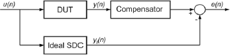
Figure 4: Post compensation scheme.
Since the DUT can be approximated by the real SDM of Fig. 2, it can be represented by a Volterra model. Now, it is known that it can also be p-linearized with a Volterra system of similar complexity (Schetzen, 1980). From Section II, we know that the Volterra representation for the SDM is more general than a Hammerstein or a Wiener model. We also know that more than one linear dynamic is needed to represent it (see Fig. 2.). Thus, the choice of a model for the compensator should be more complex that Hammerstein or Wiener models.
In this section two compensator structures are considered. The nonlinearities are described by piecewise linear (PWL) functions as presented in Julián et al. (1999). The PWL functions are defined on a rectangular compact domain S of the form
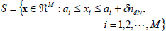 | (1) |
where  is the size of the grid and ndiv (a positive integer), is the number of divisions associated with the xi axis. The domain S is subdivided using a simplicial boundary configuration H.
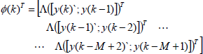
The space PWLH[S] of all continuous PWL mappings defined over the domain S partitioned with a simplicial boundary configuration H, is a linear vector space. A basis for this space can be constructed by defining each element as a function of s-nesting absolute value functions and the elements of this basis can be expressed in a vector form, according to its nesting level as
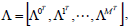
where  is the vector containing the s-nesting level functions. In this way, according to Julián et al. (1999), any nonlinear function
  can be written as
 | (2) |
where
and every vector  is a parameter vector associated with the s-nesting level vector .
A. Parallel Hammerstein with PWL static function (PHPWL)
The structure of the PHPWL model is given for M parallel branches formed by a PWL function with outputs combined linearly (Fig. 5), i.e.,
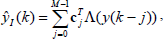 | (3) |
which can be written in the form of a linear regressor as,
 | (4) |
where
 | (5) |
and
 | (6) |
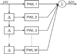
Figure 5: Parallel Hammerstein with PWL static function.
B. Parallel Wiener with PWL static function (PWPWL)
A natural structure for the PWPWL (Fig. 6) is to consider M delayed inputs to a single PWL of dimension N=M. However, this choice involves a number of parameters O(NMdiv), which makes this alternative impractical. In order to reduce the complexity of the model, we consider M-1 parallel PWL functions with two delayed inputs each, i.e.,
 | (7) |
which also can be posed in the form of a linear regressor as,
 | (8) |
where in this case
 | (9) |
and
 | (10) |
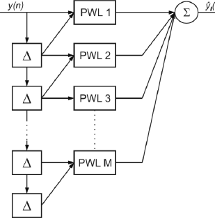
Figure 6: Parallel Wiener with PWL static function.
C. Parameter estimation.
Once the model structure has been chosen, the issue of parameter estimation arises. The values of the model parameters must be estimated in such a way that a given error criterion is minimized.
We can distinguish two phases of operation for each kind of compensator. The first one is the "training mode", in which the parameters of the model are estimated by minimization of the error between its output and a reference value (as shown in Fig. 4). The second is the "running mode", where the chosen parameters are used to predict the desired output of the model.
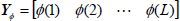
Let us define the reference value yI(k), which is the desired output of the compensator. This reference value is generated separately by simulation of an ideal SDM, using the test input signal u(t) (Fig. 4) and written in vector form as,
 | (11) |
where L samples are used for training.
On the other hand, the output of the compensator, (4) and (8) can be written as
 | (12) |
where  is the matrix of measurement data for a sequence of L samples composed by the regressor vectors, (6) and (10),
 | (13) |
and θ is the vector of parameters to be estimated.
The regressor and the parameter vectors are a function of the output of the DUT (y(k)) when it is excited by the input u(t) and depend on the model structure.
Then, in the training phase the parameters can be estimated through least squares (LS), i.e., minimizing the squared error defined as
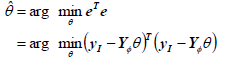 | (14) |
where the solution is given as
 | (15) |
In order to ensure the invertibility of the term  the condition of persistent excitation should be satisfied.
In the running phase, the predicted output is
 | (16) |
IV. SIMULATIONS AND RESULTS
The performance of the compensation method was simulated in MATLAB for different sets of input-output signals provided by the circuit model of the SDM. An ideal SDM was simulated in MATLAB both to estimate the parameters of the compensators and to measure their performance through the generation of the signal yI. The input signal used to excite this ideal modulator is imported to MATLAB from the circuit simulator software, so the output of both models can be compared.
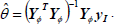
Figure 7 shows the spectrum of the input single-tone signal and the output of the DUT before and after compensation using both an PHPWL and an PWPWL as compensators. It is clear that after compensation all harmonics are significantly reduced. Furthermore, the signal to noise and distortion ratio (SINAD) was computed for the DUT before and after compensation, and compared to the theoretical result for signal to noise ratio (SNR) of an ideal distortionless SDM, showing a close to ideal behavior for the compensated SDC (Table 1).
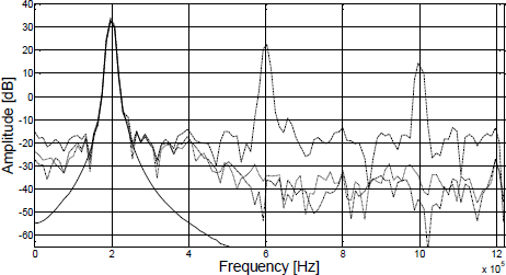
Figure 7: Spectrum of the input signal (solid line) and the output of the DUT before (dashed line) and after compensation with 5 sectors (PHPWL: dot-dash, PWPWL: dots).
The structural parameters chosen for the PHPWL compensator are a memory of M = 10 past samples from the DUT output, with a partition of Ndiv =5 sectors for the PWL static functions. This gives a total amount of 55 parameters. For the PWPWL the memory is M = 10 with a partition of Ndiv =5 for a total of 324 parameters. We consider a larger memory because high frequency signal components (above the 200 kHz tone) introduce longer memory effects. The experiment was repeated for both models increasing the number of sectors to Ndiv =10, which gives a total amount of 110 parameters for the PHPWL model and 648 parameters for the PWPWL. The results (see Fig. 8.) show a similar performance. With respect to the number of sectors on the division, it should be considered that the number of parameters grows exponentially (Julian et al., 1999) with the number of sectors. Then it is important to retain it as low as possible.
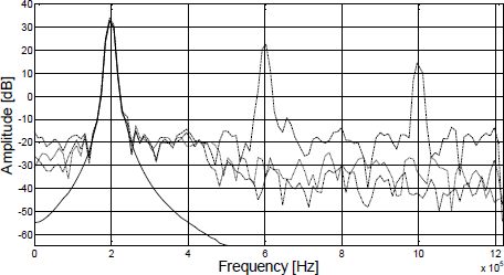
Figure 8: Spectrum of the input signal (solid line) and the output of the DUT before (dashed line) and after compensation with 10 sectors (PHPWL: dot-dash, PWPWL: dots).
The tests using single-tone signals show that a large improvement can be obtained by compensation using both models, but it is not clear which one offers a better representation for the dynamics of the system. For this purpose, a more general signal has to be used as excitation for the circuit model of the SDM. Therefore, we chose a multi-tone signal (MT) with four tones at 100, 200, 400 and 800 kHz. This signal does not only cover most of the signal bandwidth but frequencies are chosen in such a way that harmonics due to different frequency components do not overlap.
Figure 9 and Figure 10 show the spectrum of the input signal and the output of the DUT before and after compensation using both models for Ndiv =5 and Ndiv =10, respectively. We see that both models achieve a good cancelation of harmonic distortion. However, the LSE is an order of magnitude lower for the PWPWL (see Table 2). The spurious free dynamic range (SFDR) improvement obtained with the PWPWL is about 10 dB higher than that of the PHPWL. This can be explained by the presence of cross terms in the PWPWL, which allows to model the dynamics of the system in more detail, at the cost of increased complexity in terms of the amount of parameters to be estimated. In a future work we will be interested in a more precise analysis on the effect of the number of sectors in the PWL in the compesator performance. Another topic of interest for future work would be to explore the phase relations among the different sinusoids, as this may alter more complex waveforms.
Figure 9: Spectrum of the input signal (solid line) and the output of the DUT before (dashed line) and after compensation with 5 sectors (PHPWL: dot-dash, PWPWL: dots).
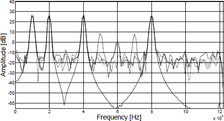
Figure 10: Spectrum of the input signal (solid line) and the output of the DUT before (dashed line) and after compensation with 10 sectors (PHPWL: dot-dash, PWPWL: dots).
Table 1: LSE and improvement in SINAD and SFDR for single tone analysis.
Table 2: LSE and improvement in SINAD and SFDR for multi-tone analysis.
V. CONCLUSIONS
This paper introduces a behavioral model for a CT SDM which justifies the use of Volterra type post-compensators. However, we show that simple Hammerstein and Wiener models are inadequate for modeling the complex nonlinear dynamics involved. Therefore, two post-compensators which are generalizations of them are developed and tested. These compensators are parallel Hammerstein and Wiener systems with PWL static functions and efficient structure to keep the amount of parameters low. The performance of such compensators is then evaluated and compared by simulations in MATLAB, using the usual metrics for ADCs such as SFDR, SINAD and LSE. As expected, the PWPWL compensator results in better cancelation of distortion when a more general input signal is used to excite the circuit.
REFERENCES
1. Björsell, N., Modeling Analog to Digital Converters at Radio Frequency, Doctoral Thesis in Telecommunications, Stockholm, Sweden (2007).
2. Bonizzoni, E., A.P. Perez, F. Maloberti and M. Garcia-Andrade, "Third-order Σ−Δ modulator with 61-dB SNR and 6-MHz bandwidth consuming 6mW," 34th European Solid-State Circuits Conference, Edinburgh, 218-221 (2008).
3. Irons, F.H., D.M. Hummels and S.P. Kennedy, "Improved compensation for analog-to-digital converters," IEEE Transactions on Circuits and Systems, 38, 958-961 (1991).
4. Jeong, T-S., W. Choi, J. Gi and C. Yoo, "Low voltage analog digital converter using sigma-delta modulator," International SoC Design Conference, Busan, III52-III53 (2008).
5. Jose, B.R., P. Mythili, J. Singh and J. Mathew, "A triple-mode sigma-delta modulator design for wireless standards," 10th International Conference onInformation Technology, Orissa, 17-20 (2007).
6. Julián, P., A.C. Desages and O.E. Agamennoni, "High level canonical piecewise linear representation using a simplicial partition," IEEE Transactions on Circuits and Systems, CAS-46, 463-480 (1999).
7. Karema, T., T. Ritoniemi and H. Tenhunen, "Intermodulation in sigma-delta D/A converters," IEEE International Symposium on Circuits and Systems, Montreal, Canada, 1625-1628 (1991).
8. Leuciuc, A., "On the nonlinearity of integrators in continuous-time delta-sigma modulators,"⋅IEEE Midwest Symp. on Circuits and Systems, Dayton, OH , USA, 862-865 (2001).
9. Lundin, H.F., Characterization and Correction of Analog-to-digital Converters, Doctoral Thesis in Signal Processing, Stockholm, Sweden (2005).
10. Morgado, A., R. del Rio, J.M. de la Rosa, F. Medeiro, B. Perez-Verdu, F.V. Fernandez and A. Rodriguez-Vazquez, "Reconfiguration of cascade sigma delta modulators for multistandard GSM/Bluetooth/ UMTS/WLAN transceivers," IEEE International Symposium on Circuits and Systems, Island of Kos, Greece, 1884-1887 (2006).
11. Nikaeen, P. and B. Murmann, "Digital compensation of dynamic acquisition errors at the front-end of high-performance A/D converters," IEEEJournal of Selected Topics in Signal Process, 3, 499-508 (2009).
12. Ryan, I. and H. Mahdi, "An oversampled rate converter using sigma delta noise shaping," IET Irish Signals and Systems Conference, Dublin, 1-6 (2009).
13. Schetzen, M., The Volterra and Wiener theories of Nonlinear Systems, John Wiley and Sons Inc., New York, USA (1980).
14. Schmidt, C., J.E. Cousseau, J.L. Figueroa, R. Wichman and S. Werner, "Nonlinearities modeling and post-compensation in continuous-time sigma-delta modulators," IET Microwaves, Antennas and Propagation, 5, 1796-1804 (2011).
15. Van de Plassche, R., CMOS Integrated Analog-to-Digital and Digital-to-Analog Converters, Kluwer Academic Publishers, Dordrecht, The Netherlands, (2003).
16. Vito, L.D., H. Lundin and S. Rapuano, "Bayesian calibration of a lookup table for ADC error correction," IEEE Transactions on Instrumentation and Measurement, 56, 873-878 (2007).
17. Yang, W-L., W-H. Hsieh and C-C. Hung, "A third-order continuous-time sigma-delta modulator for Bluetooth," International Symposium on VLSI Design, Automation and Test, Hsinchu, 247-250 (2009).
Received: April 12, 2012
Accepted: May 5, 2012
Recommended by Subject Editor: Gastón Schlotthauer and María Eugenia Torres.
